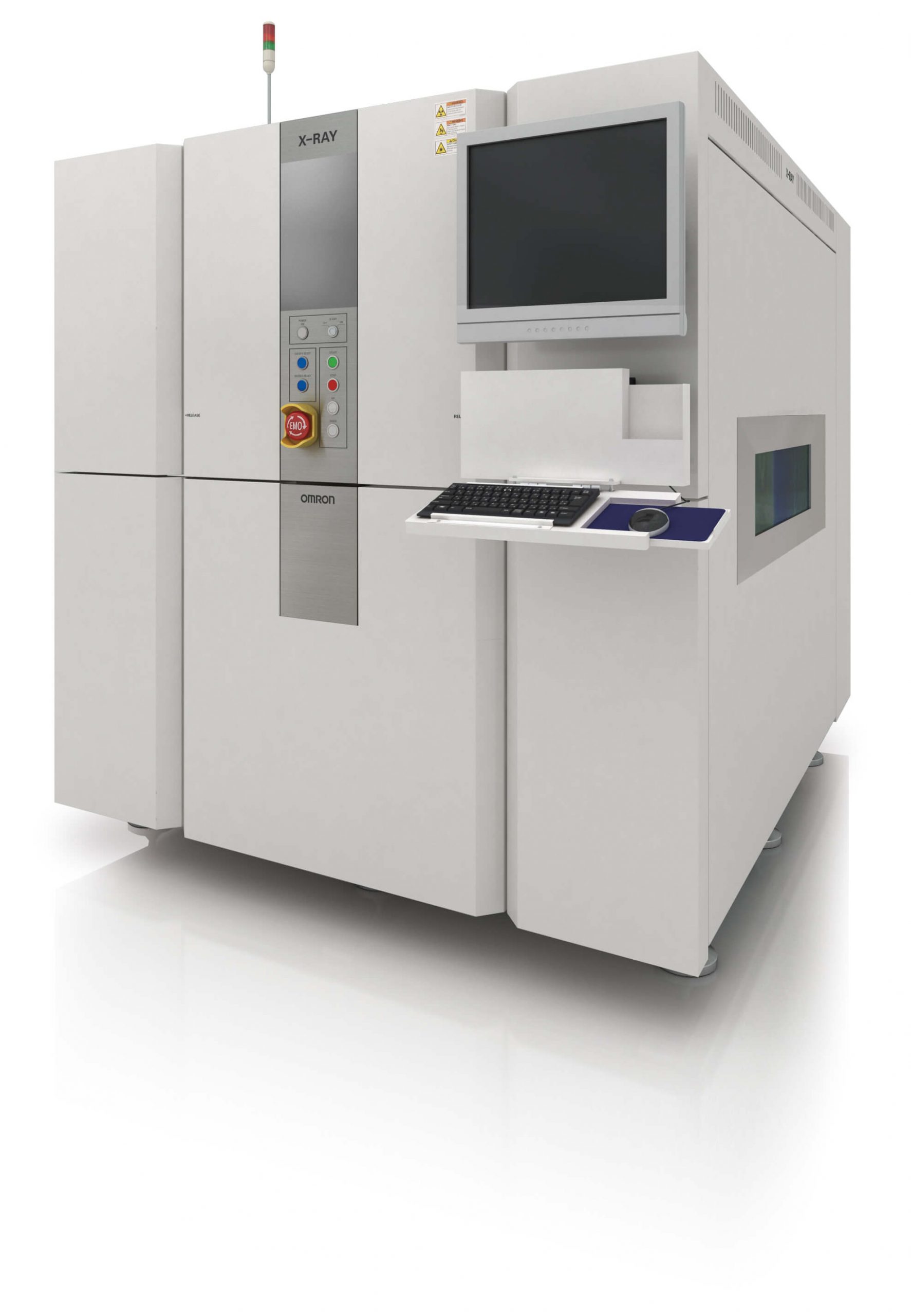
OMRON Corporation based in Kyoto, Japan, has announced the development of a new VT-X750-V3 system, the world’s fastest (*1) CT-type X-ray inspection device (*2) to date, and said it will be released globally on November 20. The VT-X750-V3 delivers advanced, true 3D inspection of electronic substrates to meet the growing needs of fifth-generation mobile communication systems (5G), electric vehicles (EVs), and autonomous driving application products. OMRON contributes to the security and safety of society through high-speed, PCB design constraint-free, 100% X-ray inspection of electronic substrate assemblies to maintain and improve productivity while simultaneously ensuring the quality of customer products.
Realizing even faster, high-quality, CT-type X-ray automated inspection with VT-X750-V3: https://kyodonewsprwire.jp/img/202111052966-O6-OLtVm6x2
In recent years, demand for electronic substrates to support 5G, EVs, and autonomous driving applications has grown rapidly, which in turn continues to raise the quality requirements of these substrates. These advanced applications may involve risks to human life and the highest-quality inspection is necessary to ensure the reliability, performance and safety of the final products. Design, manufacturing and inspection challenges are growing such as progressing PCBA densification through IC chipping, which relates to parts mounting on both sides of the board and further consolidation of parts to increase the number of components mounted on the board. To inspect these components with true accuracy and stability, traditional 2D X-ray imaging techniques are insufficient or incapable and 3D inspection has become essential. However, 3D X-ray imaging, image processing and inspection take time. It is very difficult to achieve both operating effectiveness and high-quality inspection. Historically, in order to keep pace with antiquated 2D X-ray cycle-times or meet production demands, 3D CT inspection may have only been used on a portion of the assembly, for the most critical components or in an offline inspection cell away from the production line to meet 100% inspection requirements.
Comparing X-ray technology imaging of solder defects: traditional 2D-2.5D (left) and true 3D CT (right): https://kyodonewsprwire.jp/prwfile/release/M102197/202111052966/_prw_PI1fl_RV565X3o.png
The VT-X750-V3 delivers an inspection speed 1.5 times faster than the current model, making 100% CT X-ray inspection of even complex substrates more achievable than ever. High-speed acquisition of clear 3D images has been actualized with unique, continuous imaging technology (*3) and seamless, smooth motion through OMRON’s own machine control equipment and a camera with two times (*4) the sensitivity of conventional technology. This allows for high-performance inspection within a shorter cycle time. In addition, the CT imaging condition settings used for inspection are more automated through ongoing OMRON AI development in order to further reduce program-tuning time. OMRON’s expertise, experience and continuous innovation have been helping to improve customer productivity for more than 30 years.
Today’s more complex substrates/components require 3D CT AXI: https://kyodonewsprwire.jp/img/202111052966-O2-1k04Q1rT
OMRON’s strategic concept of “innovative-Automation” consists of the three i’s: “integrated (the evolution of control),” “intelligent (intelligence developed through IoT and AI),” and “interactive (new harmonization between humans and machines).” OMRON is driving innovations on the production floor. By combining the integration of the widest range of control devices and the use of AI fully versed in solder inspection, the VT-X750-V3 is the latest offering from OMRON that embodies the “innovative-Automation” concept. OMRON offers total solutions designed to achieve zero-defect production lines.
Key features
- Achieving inspection speeds 1.5 times faster than the current OMRON system through unique, continuous imaging technology: OMRON continues to maintain high-quality imaging of 3D CT data (3D images) alongside optimized hardware control to realize inspection times 1.5 faster than the current model. This enables high-precision, 100% inspection without any compromise to productivity. To develop the advanced optimization of hardware control, OMRON concentrated in-house knowledge and expertise alongside OMRON motion control devices to actualize high-speed, seamless, continuous imaging and more accurate positioning with real-time feedback control. Through these unique and innovative technologies OMRON can deliver clear 3D CT images. Additionally, the high-speed, high-sensitivity camera combined with OMRON’s latest 3D algorithms reduce X-ray noise to even further improve overall automated inspection capability and stability.
Comparison of Omron VT-X series 3D CT AXI inspection speeds over time: https://kyodonewsprwire.jp/prwfile/release/M102197/202111052966/_prw_PI5fl_fxqN8669.png - Power device inspection OMRON has introduced new inspection logic to optimize inspection for components such as IGBT and MOSFET (*5) power devices. OMRON VT-X series 3D CT X-ray continues to be heavily utilized for solder filling inspection of through-hole connectors, inspection of press-fit connectors and inspection of SiP/PoP packages (*6), which have seen a continual increase in utilization over recent years. Inspection of power devices in particular is becoming more critical as power semiconductors are changing from Si to SIC or GaN (*7) and heat release issues are becoming more important. When facing growing EV challenges and demands for increasing mileage per charge, higher power and reductions in size and weight, heat release issues are unavoidable. OMRON has developed advanced and proprietary inspection algorithms to target the critical void inspection of solder joints to help address heat release issues.
Inspection of GaN power device (left) and SiP (right) using OMRON 3D CT X-ray imaging: https://kyodonewsprwire.jp/prwfile/release/M102197/202111052966/_prw_PI3fl_D509F0GE.png - Improving automation and reducing skill level requirements with OMRON AI: X-ray inspection frequently requires a need for the optimization of imaging conditions due to various test objects, component types or component locations on both sides of the PCB. Multiple parameters can be adjusted when setting these conditions. The conventional method was frequent, manual setting through trial and error until the optimal imaging condition is identified. However, it is now possible to automatically make these determinations with AI to significantly shorten the tuning process. 3D CT data, captured with the VT-X750-V3, need advanced and powerful technology to process 3D images. By registering the 3D image processing settings beforehand, the VT-X750-V3 is able to achieve true, automated inspection at the production site. However, the tuning of these settings may require specialized skills. New AI tools are helping to automate some of these processes; and thus reducing both the setting time and necessary skill level.
- Reducing the risk of X-ray exposure: In addition to preventing X-ray exposure to operators, reducing risk of failure due to over-exposure of semiconductor components on the products being inspected is a real concern. OMRON has developed a feature that can accurately simulate the exposure level per component, in any location and on both sides of the board. This new function reduces the risk of component failure due to excessive X-ray exposure by verifying dosage amounts.
X-ray exposure simulation per component: https://kyodonewsprwire.jp/prwfile/release/M102197/202111052966/_prw_PI4lg_OXSXT7PE.png
